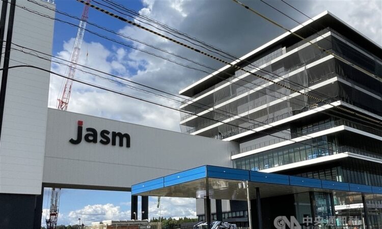
Taipei, Feb. 24 (CNA) The expansion of chipmaking giant Taiwan Semiconductor Manufacturing Co. (TSMC) in Japan will cement its lead over its peers in the global semiconductor market while also providing a major boost to Japan’s chip infrastructure, analysts said.
“TSMC is ahead of its rivals to invest in Japan, further strengthening its leadership status,” Ray Yang (楊瑞臨), a consulting director at the government-sponsored Industrial Technology Research Institute (ITRI), told CNA.
TSMC’s well-established production and research and development hubs in Taiwan have helped TSMC leave Intel Corp. and Samsung Electronics Corp. behind in the global pure play wafer foundry industry, he argued.
Adding a production hub will build on that advantage, according to Yang.
“I expect the investments in Japan will strengthen resilience of TSMC’s supply chain and become a strategic part of the chipmaker’s global expansion,” he said.
Yang said that while production costs in Japan will be higher than in Taiwan, they will be lower than in Europe and the United States.
In addition, Japan already has a complete supply chain that can meet TSMC’s needs, and the two fabs will ease clients’ concerns over political tensions across the Taiwan Strait, Yang said.
TSMC will officially open its first fab in Kumamoto in southern Japan on Saturday afternoon under a joint venture called Japan Advanced Semiconductor Manufacturing (JASM), with commercial production scheduled to begin in the fourth quarter.
Previously on Feb. 6, TSMC said JASM, which is currently owned by TSMC and Japanese partners Sony Semiconductor Solutions Corp. (SSS) and Denso Corp., will build a second fab in Kumamoto.
Construction is slated to begin at the end of this year, with operations scheduled to start at the end of 2017.
TSMC said Japanese auto giant Toyota will take a minority stake in the joint venture, with TSMC holding an 86.5 percent stake in JASM and SSS, Denso and Toyota to hold a 6 percent, 5.5 percent and 2 percent stake, respectively.
Together with JASM’s first fab, the overall investment of JASM will exceed US$20 billion to roll out chips using TSMC’s mature 40 nanometer, 28nm, 22nm, 16nm, 12nm processes as well as the advanced 7nm and 6nm technologies.
Yang said TSMC’s competitors are unlikely to venture into the Japanese market.
Intel has decided to expand production its capacity in Israel and Ireland and is building a new plant in Germany, leaving it too busy to diversify further and set up an advanced wafer fab in Japan in the foreseeable future, Yang said.
As for Samsung, it has focused on South Korea and the United States in manufacturing, Yang said, and he doubted that Samsung would open a new fab in Japan given the animosity South Korea and Japan have had for each other over the years.
“I believe TSMC will be more than welcome in Japan to build a third fab there,” Yang said.
Liu Pei-chen (劉佩真), a researcher at the Taiwan Industry Economics Database under the Taiwan Institute of Economics Research, praised TSMC for making impressive progress in opening its first fab in Kumamoto relatively quickly.
While TSMC began work on its first fab in Arizona about a year before construction began in Kumamoto, the Arizona fab is not expected to start commercial production until 2025, using the advanced 4nm process, a year behind schedule.
“The progress in the Kumamoto fab demonstrated the Japanese government’s ambition to strengthen its semiconductor industry by quickly providing mass subsidies (to JASM),” Liu said.
According to media reports in Japan, investment in the first Kumamoto plant totaled about 1.1 trillion Japanese yen (US$7.33 billion), and the subsidies provided by the Japanese government accounted for almost half of the amount.
In addition to the Kumamoto fab investment, TSMC also set up the TSMC Japan 3DIC R&D Center in March 2021.
The subsidiary, located in the Tsukuba Center of the National Institute of Advanced Industrial Science and Technology, will develop high-end integrated circuit packaging and testing services and provide one-stop services to clients.
Liu said that while Japan cannot catch up with the U.S., South Korea and Taiwan any time soon in terms of global market share, TSMC’s presence in Kumamoto is expected to advance Japan’s status in the global semiconductor world.
According to Taipei-based information advisory firm TrendForce Corp., Japan is currently focused on mature semiconductor production and taking about a 3 percent share in the global market.
TrendForce said Japan is expected to maintain a 3 percent share in global mature processes below the 28nm process and secure a 4 percent share in processes more advanced than 16nm technology in 2027.
In Arizona, TSMC is also building a second fab, using the 3nm process, the most advanced process that TSMC is currently producing commercially.
TSMC has rescheduled mass production of the second fab in Arizona for 2027, instead of 2026 the company had previously planned.
In Germany, TSMC has teamed up with Bosch GmbH, Infineon Technologies AG, and NXP Semiconductors N.V. to set up a joint venture, called European Semiconductor Manufacturing Co. (ESMC), which intends to build a wafer fab in Dresden.
The German plant is scheduled to start commercial production at the end of 2027, using the 12nm, 16nm, 22nm, and 28nm processes to produce chips for automotive electronics and specialty industrial devices.
TSMC further cemented its leading share of the global pure play wafer foundry market in the third quarter of 2023 by taking a 57.9 percent share of the market, up from 56.4 percent in the second quarter, according to TrendForce.
