(Bloomberg) — SK Hynix Inc. is ramping up its spending on advanced chip packaging, in hopes of capturing more of the burgeoning demand for a crucial component in artificial intelligence development: high-bandwidth memory.
Most Read from Bloomberg
The Icheon-based firm is investing more than $1 billion in South Korea to expand and improve the final steps of its chip manufacture, said Lee Kang-Wook, a former Samsung Electronics Co. engineer who now heads up packaging development at SK Hynix. Innovation with that process is at the heart of HBM’s advantage as the most sought-after AI memory, and further advances will be key to reducing power consumption, driving performance and cementing the company’s lead in the HBM market.
Lee specializes in advanced ways of combining and connecting semiconductors, which has grown in importance with the advent of modern AI and its digestion of vast troves of data via parallel processing chains. While SK Hynix has not disclosed its capital expenditure budget for this year, the average analyst estimate puts the figure at 14 trillion won ($10.5 billion). That suggests advanced packaging, which could take up a 10th of that, is a major priority.
“The first 50 years of the semiconductor industry has been about the front-end,” or the design and fabrication of the chips themselves, Lee said in an interview. “But the next 50 years is going to be all about the back-end,” or packaging.
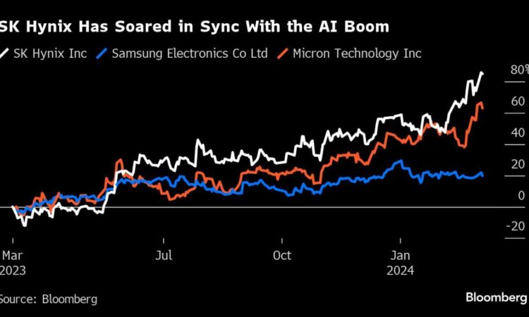
Being first to achieve the next milestone in this race can now catapult companies into industry-leading positions. SK Hynix was chosen by Nvidia Corp. to provide the HBM for its standard-setting AI accelerators, pushing the Korean firm’s value up to 119 trillion won. Its stock has gained nearly 120% since the start of 2023, making it South Korea’s second most valuable company and outperforming Samsung and US rival Micron Technology Inc.
Lee, now 55 years old, helped pioneer a novel method to packaging the third generation of the technology, HBM2E, which was quickly followed by the other two major makers. That innovation was central to SK Hynix winning Nvidia as a customer in late 2019.
Stacking chips to derive greater performance has long been Lee’s passion. In 2000, he earned his PhD on 3D integration technology for micro-systems from Japan’s Tohoku University, under Mitsumasa Koyanagi, who invented stacked capacitor DRAM used in mobile phones. In 2002, Lee joined as principal engineer at Samsung’s memory division, where he led the development of Through-Silicon Via (TSV)-based 3D packaging technologies.
That work would later become the foundation for developing HBM. HBM is a type of high-performance memory that stacks chips on top of one another and connects them with TSVs for faster and more energy-efficient data processing.
But back in the pre-smartphone era, Samsung was making bigger bets elsewhere. And the norm was for global chipmakers to outsource to smaller Asian nations the tasks of assembling, testing and packaging chips.
So when SK Hynix and US partner Advanced Micro Devices Inc. introduced HBM to the world in 2013, they remained unchallenged for two years before Samsung developed its HBM2 in late 2015. Lee joined SK Hynix three years later. They joked, with a measure of pride, that HBM stood for “Hynix’s Best Memory.”
“SK Hynix’s management had better insights into where this industry is headed and they were well prepared,” said Sanjeev Rana, an analyst at CLSA Securities Korea. “When the opportunity came their way, they grabbed it with both hands.” As for Samsung, “they were caught napping.”
ChatGPT’s release in November 2022 was the moment Lee had been waiting for. By that time, his team had developed a new packaging method called mass reflow-molded underfill (MR-MUF), aided by his contacts in Japan. The process, which involves injecting and then hardening liquid material between layers of silicon, improved heat dissipation and production yields. SK Hynix teamed up with Namics Corp. in Japan for the material and a related patent, according to a person familiar with the matter.
SK Hynix is pouring the bulk of its new investment into advancing MR-MUF and TSV technologies, Lee said.
Samsung, which has for years been distracted by a succession saga at its very top, is now fighting back. Nvidia last year gave the nod to Samsung’s HBM chips, and the Suwon-based company said on Feb. 26 it has developed the fifth generation of the technology, HBM3E, with 12 layers of DRAM chips and the industry’s largest capacity of 36GB.
On the same day, Boise, Idaho-based Micron surprised industry watchers by saying it begun volume production of 24GB, eight-layer HBM3E, which will be part of Nvidia’s H200 Tensor Core units shipping in the second quarter.
With its big commitment to expanding and enhancing technology at home and a multibillion-dollar advanced packaging facility planned for the US, Lee remains bullish about SK Hynix’s prospects in the face of intensifying competition. He sees the present investment as laying the groundwork to meet more demand to come with future generations of HBM.
Most Read from Bloomberg Businessweek
©2024 Bloomberg L.P.
